
1. What is DFM?
DFM manufacturability analysis is actually a bridge between R&D and production, communicating between them, and to make better products at a lower cost by simplifying, optimizing, and improving product design
DFM manufacturability analysis means that manufacturability is considered from the time of product development and design, so that design and manufacturing are closely linked, to achieve the goal of success from design to manufacture without any problem.
The specific situations are as follows:
- Identify potential problems during the design phase and provide solutions
- Component design error avoidance
- Make appropriate component substitutions if any chance to improve component quality or reduce costs while meeting the original needs
- Improve the productivity in production processes and component quality
- Reduce the cost of product production
2. Why is DFM so important?
The goal of the enterprise : low cost , high output , good supply capacity , and long-term reliable products . That means to produce better products with less money, and DFM can meet the needs from enterprises to a large extent. DFM is critical for efficiency, speed and high productivity.
Many people believe that about 70% of product manufacturing costs come from the initial design stage, such as materials or manufacturing, so DFM has a great ability to reduce costs. In addition, DFM can also play a role in the entire manufacturing and production process.
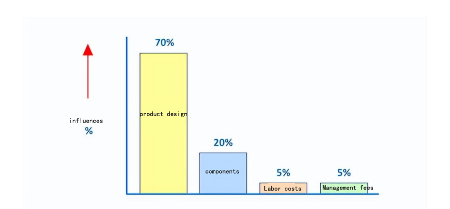
The influence map of each cycle of the product (from the Internet)
Here are a few specific points:
- With DFM, production costs can be reduced
- Accelerate the time to market
- Reduce development costs
- Reduce the number of revisions or do not require revisions, reducing development costs
- Reduce rework and rework costs
- Find errors and glitches, and avoid them
- Provide a higher quality product as the design can be improved and enhanced at each stage
From the perspective of engineers, DFM manufacturability analysis saves engineers a lot of trouble. No need to be urged by the boss, no need to stay up late to change the board, no need to bear the pressure of many parties, and can also reduce the number of times been bullied.
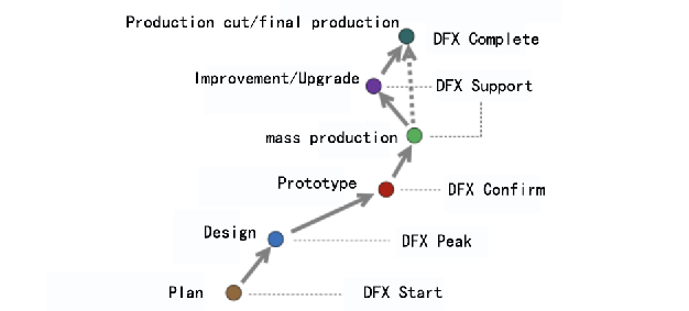
Application of DFM in each stage of product
3. What would happen without DFM?
In order to assemble printed circuit boards as quickly and efficiently as possible, it is important to design according to DFM requirements. Here are a few common problems that may arise if DFM manufacturability analysis is not performed.
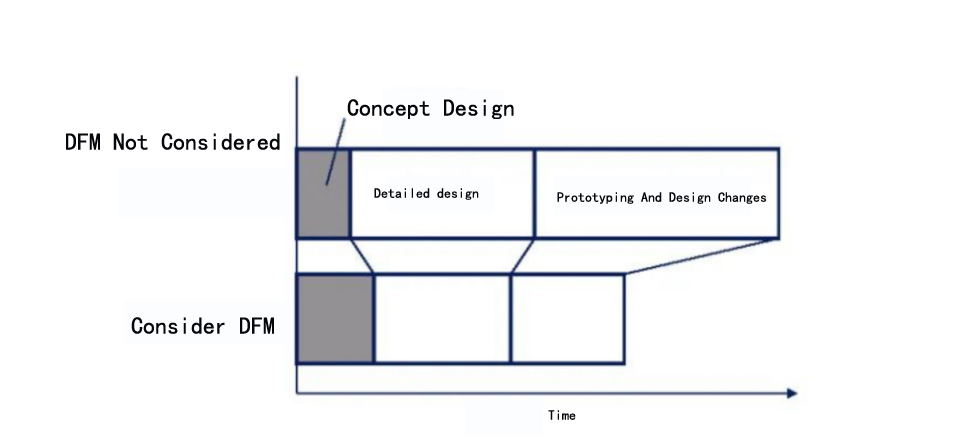
Importance of DFMs
- Haven’t done abetter choice for material price and availability
The price of electronic components may vary depending on the channel, which may have an unexpected impact on PCB assembly. Although this has little impact on the sample cost, once it is put into production, the cost will rise rapidly .
For example: if you spend $1 more on electronic components that have been used 10 times in the design, you can ignore adding $1 to one board, but if it is 10,000 boards, it will be $10,000. If all the components on the PCBA are considered, the difference of $1 will also generate a huge cost difference.
This is just a example, but in more cases, the board may be far more than 10,000 pieces.
Of course, not only the price, different suppliers and distributors will also have different changes in the application of components . If the price of the material is low, but it is not available during production, it may face huge manufacturing delays.
Especially at the end of the product production cycle , if the material is marked as not meeting the new design, service life is not up to standard, or obsolete, it is necessary to redesign the circuit board to adapt to the updated material, and may have to stay up all night to change the board .
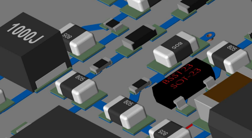
patch map
- PCBA assembly failed
If the material does not match the PCB, it will cause many errors in the manufacturing process. Here are a few common ones:
| Bad solder joint | Components that are not properly rotated for wave soldering can create bad solder joints, which may happen to the via holes and surface mounted(SMT) components. The position of components is also important, because some components may prevent good solder from being used to the other parts, causing worse connection. |
| Solder Bridge | Surface mounted pins that are very close may have a thin strip of solder between them. These solder strips may cause intermittent shorts that are difficult to find and correct. |
| Tombstone | Discrete SMT parts that are thermally unbalanced between their pins may have problems going through a reflow oven, this imbalance can pull out one of the pins and pull the part up until it stands upright like a tombstone. |
| Floating Parts | If the pad size is wrong, reflow SMT components may float misaligned, which may cause interference with other circuits |
Of course, here are just a few, in fact there will be more problems, any materials that cannot be matched correctly may need to be manually soldered or even redesigned, which means slowing down the manufacturing speed of the circuit board and spending more time and money.
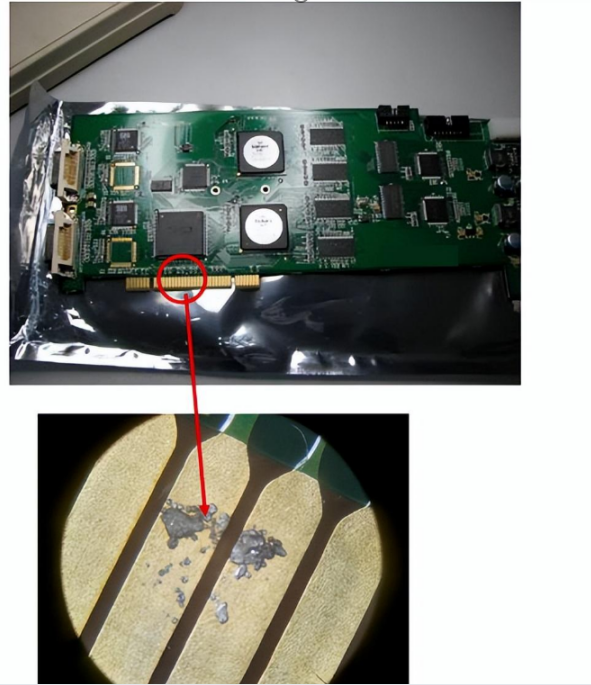
Tin dipping chart of gold finger (picture comes from the Internet)
- Reliability design
Designing for reliability is also a common problem where circuits are designed without consideration for PCB assembly and practicability. Assuming that the product is used outdoors, it must be resistant to high temperature, but it was not considered at all during the design. Such a product did not meet the standard at all during the test, and then began to redesign, select materials, and other questions may appear in subsequent production.
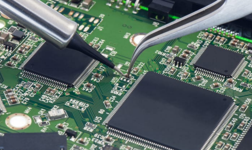
Manual welding component diagram
4. How to apply DFM in product production?
- Start with the schematic diagram
When designing the schematic diagram, the designer will choose the required materials , usually based on the function to be realized, but many other factors must also be considered, including the price , reliability and life cycle of the material . If you start thinking about it at the design stage, it will save a lot of trouble, and avoid the trouble of the manufacturer.
Here I have to talk about BOM. There are many matching materials on the market, which can actually solve a lot of problems.While there will be a little bit trouble when it comes to the production stopped, you need to consider the alternative selection.
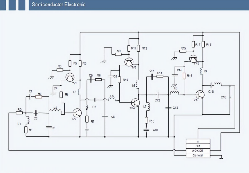
schematic diagram
- PCB layout
PCB layout is also an important part of design, and in the early stages of design, important decisions about how to set up the board also directly affect how the board is manufactured.
- Single-layer board, double-layer board or multi-layer board?
Two-layer boards are usually used for signal integrity and thermal management , while also considering the manufacturability of the board . For example, determining the board thickness required for the vias used with the optimum drill aspect ratio, which requires using a different board material or changing the number of layers of the board.
- Circuit Board model outline
Determine the model and outline of the PCB, requiring detailed circuit board shape and size , including placing fixed components, through holes , slots , etc. Care must be taken here so that redesign and assembly errors can be avoided.
- Materials
To avoid soldering problems during assembly , it is necessary to have the materials ready.
- Place and route according to DFM requirements
PCB component placement and routing requires layout with the shortest signal paths in high-speed and power circuits for best electrical performance. When laying out a board , it is important for the PCB designer to strike a balance between the electrical and manufacturing needs of the board .
Mainly pay attention to the following points:
|
Points to note |
Description |
| SMT |
In order make the chip mounter automatically assemble components, it is necessary to keep a certain distance between the components. Of course, manual soldering cannot be avoided sometimes.
|
| Wave soldering |
Both the DIP and SMT components need to be placed perpendicular to the direction of the circuit board through the solder wave, which is conducive to the even distribution of solder around the component pins. The placement of the DIP components will also affect the solder. For example, when the DIP and SMT components are on the same side of the PCB, reflow soldering will be performed before wave soldering. |
| Reflow soldering |
The two pins of a smaller discrete SMT part need to be thermally balanced for reflow soldering. When a pad is connected to large area metal, it can act as a heat sink and cause the solder paste on that pad to reflow more slowly than the other pad, causing part tombstoning. Pad size is also a problem, as pads that are too large may cause parts to float out of alignment, while pads that are too small may not hold enough solder paste to reflow into a solid connection.
|
| PCB Package |
Vias that are too large for their pins can scatter solder through them too quickly, resulting in poor solder connections. SMT pads that are too large may contain too much solder paste, which can bridge to adjacent pads and cause shorts. Pads that are too close together are also prone to solder bridging. This often occurs in fine pitch components where there is not enough solder layer between pads to prevent bridging. |
- Design finalization and documentation
In addition to place and route, there are many other tasks during PCB layout that affect board manufacturability:
| Points to note | Description |
| PCB Testing | To verify the accuracy of the assembly process, circuit boards often include test points accessible to the probes of the test fixture. However, if test points were not included in the original design, the board must be redesigned to add them before it can go into production. A redesign like this is not only costly and time consuming, but it may also generate new DFM issues that didn't exist before. |
| Silkscreen and PCB marking | Silkscreen marking is important for PCB testing, rework and debugging. If the necessary information is not on the board, manufacturing can be slowed down,meanwhile rework and testing technicians need to look for specific parts or polarity markings. |
| Design summary drawing | Without complete and accurate information on design revisions, time may be wasted when verifying manufacturing details, or even worse, errors can be made during board production. |