
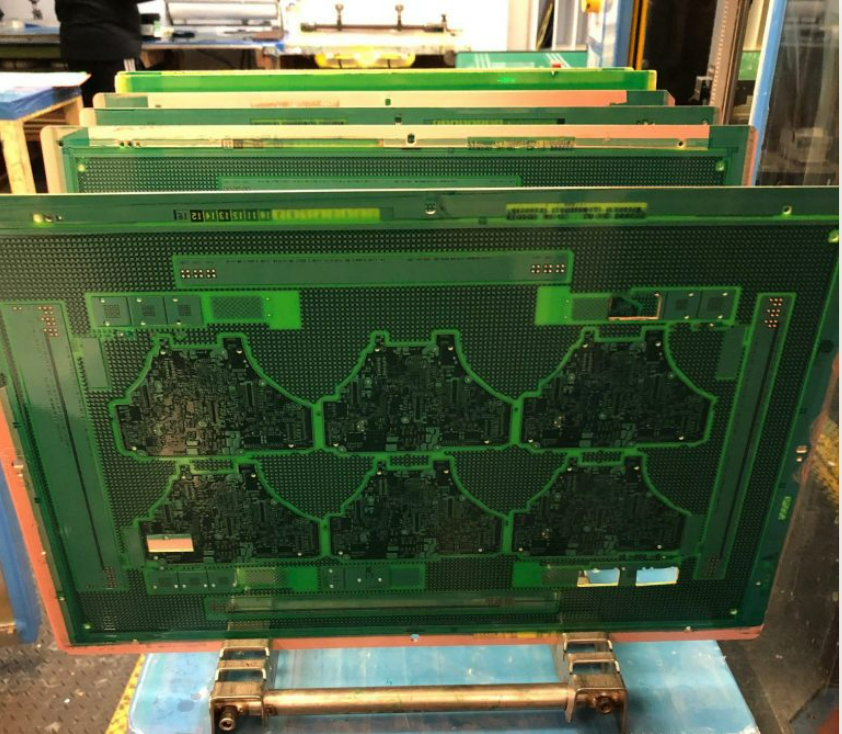
Solder mask is a layer of PCB oil that covers copper and PCB material to insulate and protect the outside surface of the PCB from short circuits and the environment. Opening windows are necessary on the solder mask to allow the PCB pads to be soldered or connected and enables heat dissipation for some vias that are not covered with PCB ink. These openings on the solder mask are solder mask openings.
During PCB design, you should be aware that solder masks are those empty areas without electronic components. During the production, these blank areas are printed with green, black, white or other PCB inks. The solder mask opening is to remove the paint layer on the circuit, which gets the tin exposed on the circuit.
Technique for Solder Mask Opening
1.The solder mask opening of the PCB pads
PCB pads are used to connect surface mounted electronic components, such as resistors, capacitors, ICs, etc. Therefore, PCB pads should not be printed with PCB ink, which means when you design the printed circuit board, you should create a solder mask opening for each PCB pad in the solder mask.
2.Solder Mask Opening of PCB Through Hole
Whether PCB through holes require solder mask openings depends on the needs of your printed circuit board. Normally you can design solder mask openings for PCB through holes for better heat dissipation. Especially for power PCBs that carry large currents, solder mask openings for heat dissipation are widely applied.You can also fill the solder mask openings with tin, which acts as a metal heat dissipation.
Solder mask openings for PCB through-holes can also be used as PCB test points due to the exposure of copper.
The above are the two purposes for PCB through solder mask openings. Besides, PCB through hole can also use solder mask to protect copper from oxidation, especially in corrosive environments.
3.Solder Mask Opening of Gold Finger
PCB gold fingers are a row of exposed hard gold-plated pads on the edge of the PCB for plugging and connecting. Solder mask openings are necessary for gold fingers because solder mask is insulating and gold fingers are used for connection and need to have excellent conductivity.
Without solder mask, you don't need to worry about the oxidation of gold fingers. Surface finishing, hard gold plating protects the copper pads well.
4.Solder mask opening for groundingpoint
You can design solder mask openings for the PCB grounding point, and the exposed copper can be connected to the metal case.
5.Solder mask opening for copper thickness measurement
In the PCB manufacturing process, we need to measure the copper thickness of the PCB to see if it is qualified.
6.PCB antenna solder mask opening
PCB antennas transmit and receive RF microwaves and consume a lot of power. For high frequency PCBs, solder mask openings for PCB antennas are common because the antenna can dissipate less power.
Solder mask opening design
1.Dimension design
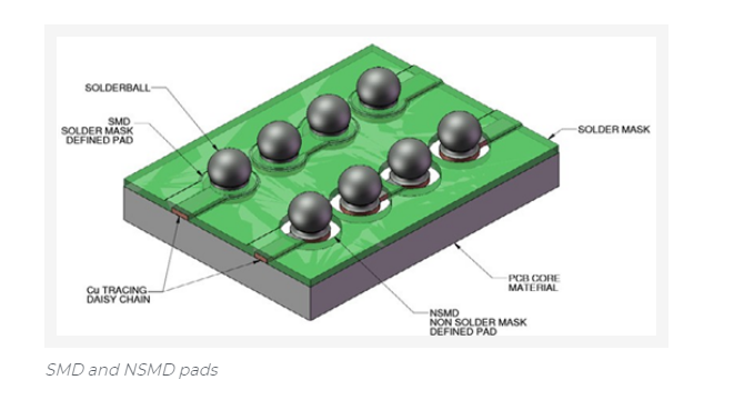
During PCB fabrication process, the solder mask opening size should be larger than the size of pad or copper area that are supposed to be exposed.
The PCB oil around the solder mask opening will melt together and the exposed area will be smaller. Typically, the size of the solder mask opening is 4 mils larger than the pad.
Is it necessary to set the solder mask opening size during PCB design? No, you just need to keep the same size as the pads/vias that are supposed to exposed, since the EDA tool will automatically enlarge the solder mask opening size.
2.PCB solder mask opening method
In PCB design, the solder mask opening can be set on the top and bottom sides of solder mask layers.
Top and bottom solder mask green oil layer: The solder mask green oil of both top and bottom sides is used to prevent tin from getting on copper foil and maintain insulation. Solder mask opening can be placed on this layer to pads, vias, and non-electrical traces.
- In the PCB design, the pads will be openedby default (OVERRIDE: 0.1016mm), that is, the pad exposes the copper foil and expands by 0.1016mm. During the wave soldering process, it is recommended not to make any design changes to ensure solderability.
- In the PCB design, the vias willbe opened by default (OVERRIDE: 0.1016mm), that is, the vias expose the copper foil, enlarge by 0.1016mm and will be wave soldered with tin. If the design is to prevent solder paste from sticking to solder mask, you must select the penting option of solder mask to turn off solder mask.
- In addition, non-electrical tracescan also be puton this layer separately, so that the green oil can be blocked and the windows can be opened accordingly. If on the copper foil trace, it will be used to enhance the overcurrent capability of the conductive trace. Tin will be added during the soldering process.
If using a non-copper trace, typically used for logo and special character screen printing, you can omit it to create a character silk screen layer.